- 您现在的位置:买卖IC网 > Sheet目录345 > NCP1605FORWGEVB (ON Semiconductor)EVAL BOARD FOR NCP1605FORWG
NCP1217, NCP1217A
Latchoff
Adj
1
+
--
Comparator
HV
8
+
--
3.1 V
Set
Latch
Reset
UVLO
HV Current
Source
FB
2
80 k
1.1 V
+
--
Skip Cycle
Comparator
Internal V CC
UVLO High and Low
NC
7
24 k
Current
Sense
3
250 ns
L.E.B.
65--100--133 kHz
Clock
Set
Reset
Q Flip--Flop
DCmax = 74%
Reset
Q
Overload
Management
V CC
6
19 k
Ramp
Compensation
20 k
57 k
+
--
Ground
4
+
--
V REF
25 k
1V
1ms SS*
? 500 mA
Drv
5
* Available for “A” version only
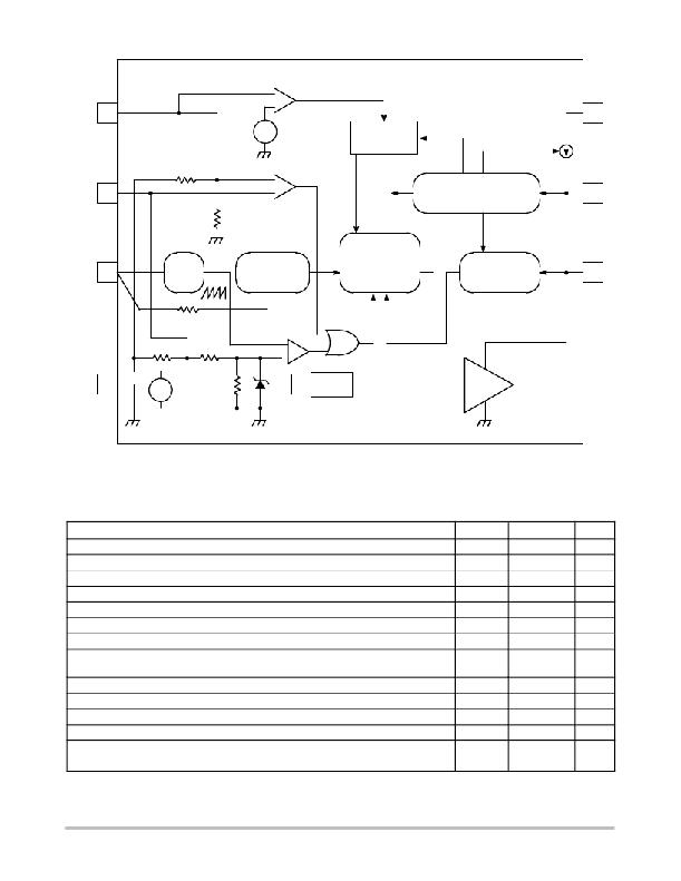
Figure 2. Internal Circuit Architecture
MAXIMUM RATINGS
Rating
Power Supply Voltage
Power Supply Voltage on All Other Pins Except Pin 8 (HV), Pin 6 (V CC ) and Pin 5 (Drv)
Maximum Voltage on Pin 8 (HV), Pin 6 (V CC ) Decoupled to Ground with 10 m F
Maximum Voltage on Pin 8 (HV), Pin 6 (V CC ) Grounded
Minimum Operating Voltage on Pin 8 (HV)
Maximum Current into All Pins Except V CC (6) and HV (8) when 10 V ESD Diodes are Activated
Thermal Resistance, Junction--to--Case
Thermal Resistance, Junction--to--Air, PDIP--7 Version
Thermal Resistance, Junction--to--Air, SO--8 Version
Maximum Junction Temperature
Temperature Shutdown
Hysteresis in Shutdown
Storage Temperature Range
ESD Capability, HBM Model (All Pins Except V CC and HV)
ESD Capability, Machine Model
Symbol
V CC
--
V HV
V HV
--
R θ JC
R θ JA
R θ JA
T JMAX
--
--
--
--
--
Value
16
--0.3 to 10
500
450
28
5.0
57
100
178
150
155
30
--60 to +150
2.0
200
Unit
V
V
V
V
V
mA
? C/W
? C/W
? C
? C
? C
? C
kV
V
Stresses exceeding Maximum Ratings may damage the device. Maximum Ratings are stress ratings only. Functional operation above the
Recommended Operating Conditions is not implied. Extended exposure to stresses above the Recommended Operating Conditions may affect
device reliability.
http://onsemi.com
3
发布紧急采购,3分钟左右您将得到回复。
相关PDF资料
NCP1840Q8A6MNTWG
IC LED DRIVER 12CH PROGR 20QFN
NCP1910GEVB
BOARD DEMO NCP1910DEMO-B-TLS
NCP3418BMNR2G
IC MOSFET DRIVER DUAL 12V 10-DFN
NCP3418DR2
IC MOSFET DRIVER DUAL 12V 8-SOIC
NCP3420DR2G
IC MOSFET DRIVER DUAL 12V 8-SOIC
NCP3488DR2G
IC MOSFET DRVR DUAL 12V 8-SOIC
NCP5007SNT1
IC LED DRIVR WHT COMPACT 5TSOP
NCP5008DMR2
IC LED DRVR WHT BCKLT 10MICROSMD
相关代理商/技术参数
NCP1605LCDTVGEVB
功能描述:BOARD EVAL NCP1605/1396 RoHS:是 类别:编程器,开发系统 >> 评估演示板和套件 系列:* 产品培训模块:Obsolescence Mitigation Program 标准包装:1 系列:- 主要目的:电源管理,电池充电器 嵌入式:否 已用 IC / 零件:MAX8903A 主要属性:1 芯锂离子电池 次要属性:状态 LED 已供物品:板
NCP1606ADR2G
功能描述:功率因数校正 IC PWR FCTR CONTROLLER RoHS:否 制造商:Fairchild Semiconductor 开关频率:300 KHz 最大功率耗散: 最大工作温度:+ 125 C 安装风格:SMD/SMT 封装 / 箱体:SOIC-8 封装:Reel
NCP1606APG
功能描述:功率因数校正 IC LO CST PWR FCTR CONT RoHS:否 制造商:Fairchild Semiconductor 开关频率:300 KHz 最大功率耗散: 最大工作温度:+ 125 C 安装风格:SMD/SMT 封装 / 箱体:SOIC-8 封装:Reel
NCP1606BDR2G
功能描述:功率因数校正 IC PWR FCTR CONTROLLER RoHS:否 制造商:Fairchild Semiconductor 开关频率:300 KHz 最大功率耗散: 最大工作温度:+ 125 C 安装风格:SMD/SMT 封装 / 箱体:SOIC-8 封装:Reel
NCP1606BOOSTGEVB
功能描述:电源管理IC开发工具 OSPI NCP1606 100 W BOOST
RoHS:否 制造商:Maxim Integrated 产品:Evaluation Kits 类型:Battery Management 工具用于评估:MAX17710GB 输入电压: 输出电压:1.8 V
NCP1606BPG
功能描述:功率因数校正 IC LO CST PWR FCTR CONT RoHS:否 制造商:Fairchild Semiconductor 开关频率:300 KHz 最大功率耗散: 最大工作温度:+ 125 C 安装风格:SMD/SMT 封装 / 箱体:SOIC-8 封装:Reel
NCP1607BDR2G
功能描述:功率因数校正 IC CST EFCT PW FCTR CTR RoHS:否 制造商:Fairchild Semiconductor 开关频率:300 KHz 最大功率耗散: 最大工作温度:+ 125 C 安装风格:SMD/SMT 封装 / 箱体:SOIC-8 封装:Reel
NCP1607BOOSTGEVB
功能描述:BOARD EVAL NCP1607 100W BOOST RoHS:是 类别:编程器,开发系统 >> 评估演示板和套件 系列:* 标准包装:1 系列:PCI Express® (PCIe) 主要目的:接口,收发器,PCI Express 嵌入式:- 已用 IC / 零件:DS80PCI800 主要属性:- 次要属性:- 已供物品:板
